Ok this is awesome. Not surprised as @IBMResearch has been cranking out semiconductor “firsts” for decades. $IBM https://t.co/n26XDCjoem
— Patrick Moorhead at #DellTechWorld (@PatrickMoorhead) May 6, 2021
In the processor improvement push, @IBMResearch has next-next-gen transistors working: nanosheets and gate-all-around. Now it just needs a partner to make chips with it in 2024 or 2025. IBM calls it a 2nm process, but take that label with a grain of salt. https://t.co/VrU58sXcHI
— Stephen Shankland (@stshank) May 6, 2021
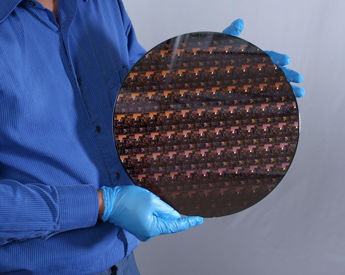
There's plenty of room in that wafer - IBM creates the world's first 2nm chip technology.https://t.co/Qv8I3OENbA pic.twitter.com/lHLSQUGShK
— OC3D (@OC3D) May 6, 2021
Very timely @IBM announcement focusing on the 2nm breakthrough as much as their US-based innovation https://t.co/ymqqfpSAoW
— Carolina Milanesi (@caro_milanesi) May 6, 2021
This is humbling m. As a scientist and professor of Elecyrical Engineering, I teached in the late 80's that the ultimate limit for IC was 5nm. I had so many reasons for being convinced that I could have bet a fortune on this!
— Nicolas Demassieux (@ndemassieux) May 6, 2021
Science and technology are always full of surprises.
Good breakdown of what 2nm means in this context by @IanCutress as such transistor descriptions are effectively marketing terms rather than a reference to true measurements. https://t.co/oKGKs32Kmw
— Leo Kelion (@LeoKelion) May 6, 2021
It was a pleasure talking with Stephen, and the article is fantastic! Great work on an inflection point in semiconductors - moving from FinFET to gate-all-around! Kudos to the IBM team for an R&D debut. But we need GAA in production for future CPUs, GPUs, SoCs, etc. https://t.co/bxODoQEp5C
— David Kanter (@TheKanter) May 6, 2021
IBM Creates First 2nm Chip https://t.co/fbKtZHdzaH Crazy amount of transistor density. What will happen after a 1nm chip? No one has demonstrated this is possible yet.
— nixCraft (@nixcraft) May 6, 2021
IBM announces the production (of a research prototype) 2nm chip with stacked GAAFETs https://t.co/5T8u3ngGpD
— Bharath Ramsundar (@rbhar90) May 6, 2021
Important update on America losing the global semiconductor race: "IBM Creates First 2nm Chip" https://t.co/pXz14LqWsa
— Scott Lincicome (@scottlincicome) May 6, 2021
"The chip was designed and made at IBM’s Albany research facility, which features a 100,000 sq. ft. clean room." pic.twitter.com/y2BrGxY7IE
Good breakdown of what 2nm means in this context by @IanCutress as such transistor descriptions are effectively marketing terms rather than a reference to true measurements. https://t.co/oKGKs32Kmw
— Leo Kelion (@LeoKelion) May 6, 2021
#IBM creates first 2nm chip
— George Mastropavlos (@g_mastropavlos) May 6, 2021
Every decade is the decade that tests the limits of Moore’s Law, and this decade is no different.https://t.co/52CAnHA8Yt pic.twitter.com/wn0NMoISYR
=>
— OGAWA, Tadashi (@ogawa_tter) May 6, 2021
"IBM Creates First 2nm Chip", May 6, 2021 https://t.co/mvrCFjHLKh
Comparison:
IBM, TSMC, Intel, Samsung
"IBM Chips In To Drive 2 Nanometer Semiconductor Manufacturing" https://t.co/4iRpuHASuY
Mukesh Khare, IBM
Three Nanosheets to the 2 Nanometer Windhttps://t.co/Xdb6FSn17J pic.twitter.com/YXxkcjgqpc
This advance was made possible by @ASMLcompany equipment. Only firm currently capable of making the machines necessary to make such tiny tech. A lot rests on the shoulders of the Dutch business. https://t.co/WVllwP7xOO
— Leo Kelion (@LeoKelion) May 6, 2021
IBM chips in research to help Samsung and probably Intel get to 2 nanometer processes out the door in 2024 for semiconductor manufacturing https://t.co/HqOj9l8L4o
— Tim Prickett Morgan (@TDaytonPM) May 6, 2021
Woah. How low can we go?!
— Andrey Kurenkov ? (@andrey_kurenkov) May 6, 2021
But really though. https://t.co/ob0rrpO40L
Intelの存在意義が皆無になってしまうぞ。 IBM says it has created the world's first 2nm chip https://t.co/F6pcEFMsw8 via @engadget
— へたれ?? (@_sushiy) May 6, 2021
IBM says it has created the world's first 2nm chip https://t.co/86PHQImBhd #tech #feedly #cpu #chip
— Nicolas Babin #AdobePartner (@Nicochan33) May 6, 2021
IBM, 세계 최초 2nm 칩 만들었다고 주장
— Wan Ki Choi (@wkchoi) May 6, 2021
- 2nm 칩은 7nm 칩 대비 같은 성능에 전력을 75% 덜 사용하고 혹은 같은 전력 사용에 성능은 45% 제고되며 손톱 하나 칩 크기에 500억개 트랜지스터를 장착
- 따라서 2nm 프로세서는 더 나은 성능과 개선된 전력효율 조합을 제공할 것https://t.co/CoituYyz4a
IBM says it has created the world's first 2nm chip - The architecture can help processor makers deliver a 45 percent performance boost with the same amount of power as current 7nm-based chips. https://t.co/P2OO85Z3ew via @engadget
— Pasquale “PJ” Catalano (@psqlctln) May 6, 2021
IBMが世界初の2nmプロセスでのチップ製造に成功!
— Daigo Wakabayashi (@frnk) May 6, 2021
TSMCが5nmで一人勝ち状態かと思ってたら、思わぬところに伏兵が。しかも一気に2nm。かつての巨人・IBMの凄さよ。 https://t.co/smh6cKPN8j
A well written and informative discussion on the new 2 nm chip and comparison to other chip technologies https://t.co/pStLNfs8nY pic.twitter.com/2ToYpxGuGF
— Kourosh Kalantar-Zadeh (@K_KalantarZadeh) May 6, 2021
プロセスが2Dのときはその定義でも(ゲートの寸法かメタルの寸法かの議論はあっても)プロセスルールの密度を表現できましたが、FinFET や GAA FETの様な3D構造だと何を示しているのか一意に定まりません。
— EGUCHI Osamu (@eguchi3) May 7, 2021
Anandtech の記事によると「等価な2Dトランジスタ相当」https://t.co/v1PC353kn4
IBMが世界初の2nm半導体技術を発表。https://t.co/biygTt65ur
— かも (@R3000C) May 7, 2021
第2世代のナノシート技術が使われているそうで(第1世代はSamsungのか)、トランジスタ密度ではオーパーツ臭のあるTSMCの3nmを上回ってる。
IBMはファウンドリは売ったけどプロセス開発は続けてたんですね。
顧客はSamsungしか無いけど。 pic.twitter.com/HB0cNH1pRT
IBM has just created a proof-of-concept chip with a 2NM process. IBM's published density numbers for this node are 333M transistors per square millimeter, whew! They say 2NM will improve performance by 45% at the same power. #IBMhttps://t.co/lD7I9gS4pL
— Jeff Duntemann (@JeffDuntemann) May 6, 2021
China has a lot of catching up to do. Whilst it prepares to produce 7nm, IBN has now broke through to 2nm.https://t.co/zLfHAtGfg2
— Tom Fowdy (@Tom_Fowdy) May 7, 2021
I remember being excited when the 20nm barrier was broken - now the talk is 2nm. Amazing!!https://t.co/xQrY31DZCg
— Prof Marc Tennant (@MarcTennant) May 7, 2021
The era of 2nm transistors
— Kourosh Kalantar-Zadeh (@K_KalantarZadeh) May 6, 2021
“IBM says it has created a 2nm chip in its test lab. It also claims its test chip can improve performance by 45% over current 7nm products. It is also more energy efficient - using 75% less energy to match current performance.”https://t.co/ssiJZHVoiI
IBM、世界初の2nmチップを製造したと発表
— Si@高校生/カメラ/テックニュース (@komyusyou_pc) May 6, 2021
このアーキテクチャにより、プロセッサメーカーは、現在の7nmベースのチップと同じ電力で45%の性能向上、または75%少ないエネルギーで同レベルの性能を実現することができる。
IBM says it has created the world's first 2nm chip https://t.co/SqM87HHfc2
IBM says it has created the world’s first 2nm chip. Suck it, China. https://t.co/5ctB41XIpL
— The Panic (@Gunntwitt) May 7, 2021
"IBM says it has created the world's first 2nm chip
— Roger Chang (@jollyroger) May 6, 2021
The company claims 2nm processors can use 75 percent less power than 7nm-based CPUs for the same performance."https://t.co/you9f08IL4
.png)